Research Activities
Many applications require the handling of objects with nanometer precision. The best example is the microsystem technology (MST). Conventional robots are not suited for the assembly of microsystems. Therefore, versatile, automated nanohandling systems with smart robots, grippers, sensors, control and planning techniques are regarded as a key technology for mastering the MST on an industrial basis.
During the last years the field of manipulation, characterization and processing of nanomaterials has become one of the main research topics in material science and nanotechnology. The extraordinary physical properties of novel nanomaterials enable numerous applications.
Automated Processing, Characterization and Manipulation at Nanoscale

We are working with nanomaterials referring to structures with nanometer sizes in at least one dimension: monolayered sheets of carbon, so-called graphene, is the best-known example for two-dimensional nanostructures, while nanotubes and nanowires made of different materials, such as Au, Si, and ZnO, are fascinating one-dimensional structures in which carbon nanotubes (CNTs) are the most prominent example. In addition to these synthesized materials our group is working on biomaterials such as DNA and wood fibers. These nanomaterials provide a basis for novel actuator and sensor technologies and can improve existing electronic devices, aiming primarily at nano-electro-mechanical systems (NEMS).
To optimize the nanomaterials’ fabrication techniques and allow the assembly of prototypic devices, reliable manipulation, characterization and flexible processing of these nanomaterials is required. In this area, the micro-nano-integration of these nanomaterials into existing microsystems remains a challenge. Automated nanorobotic systems are one of the most promising enabling technologies for this challenge closing the gap between bottom-up and top-down approaches. Our group develops and applies nanorobotic strategies for the manipulation, characterization and processing of nanomaterials bringing them one step closer to their potential applications.
Microwave-Nanoscopy and Automation at Nanoscale

Research on “beyond CMOS” requires smart tools to investigate, manipulate and transport materials, objects and systems in the nanoscale range. One crucial part along these track is imaging and characterizing the electric and dielectric properties in the microwave region of the electromagnetic spectrum. With our nanorobotic approach we working on new instruments measuring electric parameters in the GHz region.
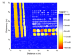
The self-developed Scanning Microwave Microscope is integrated into a Scanning Electron Microscope (SEM2). This world-first technology is the fundamental part of the aspired Nanorobotic Microwave Probing and Manipulating System (NMPMS) for Wafer-level testing of nanoelectronic and/or 3D heterogeneous nanodevices. Precise positioning of an RF probe, scanning the region-of-interest (in contact and/or near-field), is necessary to ensure high repeatability of the high-frequency measurements.

